So now you have the cube all wired up, it’s time to direct our attention to the actual prototype board. This is going to become the actual brain of the LED cube. It is not that difficult top build, but you need some basic knowledge of electronics to get it right.
If you want to do this properly for a final design, it would be best that you do your own etching of the board and place the chips and other components on there, so you’ll end up with a print like the on you find in your laptop, for example. However, that takes some additional skills and money as well. If I were to sell my LED cube I’d do it, but for my own personal POC use, the prototype board will do just fine.
Building the brains: soldering the components
The first and most important thing you need to do is to determine the actual layout of all the components. This means you’ll have to place all of the components on the board without soldering them, just to make sure your layout leaves enough space to have all the components on there. It would be a shame soldering all of the components on there only to find out in the end you don’t have enough room left for the last couple of resistors or ICs :-S.
Once you are sure you have a correct layout, you are best off starting with the IC sockets for the 74HC574 ICs and the 100 Ohm resistors, together with the male pin headers. These will be connected to the LED cube and every latch IC will be connected to one of the UTP cables you prepared in the previous step. That means that every LED you will turn on will be have a 100 Ohm resistor in its electric circuit. After soldering them in place, your board should look like this.

Next up are the transistors that will control the layers. Each 2N2222 transistor is rated for about 800mA, which is not enough, since it will receive the current from maximum 64 LED at the same time. Since the LEDs can go to 20mA each, that means that the transistor would get 1280mA and be fried in seconds. That is why I’m placing an additional transistor for each layer in parallel, so each layer will be turned on by 2 2N2222 transistors in parallel to split the current.
Simply put, each transistor can be seen as an electronic switch. For the NPN type of transistor you can compare it to a normally closed contact. If you supply power to it, the contact will allow the current to pass through. Otherwise not. Now, the transistor actually needs a separate circuit to trigger the switch and this circuit needs a 120 Ohm resistor in this case, to allow the maximum amount of current (20mA) to flow through the LEDs in the cube.
I’ve connected 2 transistors and resistors in parallel by outlining them on the same rows on the prototype board. For the transistor, you need to bent the base leg a little to have all 3 legs in 1 line. So, you end up with a resistor connected to the middle leg and you just mirror the situation on the same line. This allows a small wire to connect both resistors in the middle.
Then you connect the collectors and then the emitters of both transistors. And since we have 8 layers to play with, you’ll need to repeat this 7 more times. Last but not least, you need to connect the collectors of all 8 layers to another pin header to allow the UTP from the layers to connect to these transistors. The end result in soldering can be seen in the following image.

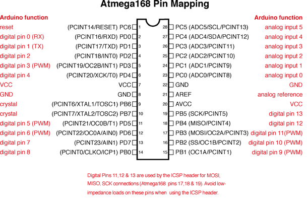
In the next step you are going to add the 74HC138 clock chip as well as the Arduino powered ATMega328, together with its crystal and 22pF capacitors. Please use the image below to connect the proper components to the proper output ports on the ATMega328 chip.
In the next images you can also see some additional soldering in place to connect the VCC line and ground to the different components. In the top view you can see some wires running on the top of the board. This is necessary because the VCC line sometimes has to cross the ground line and this is why we need these wires. In the same image you can also see there are also some additional capacitors in place to regulate the current throughout the board.
There is a 1000uF, a 100uF and a 10uF capacitor right behind the power input to get rid of the ripples in the 5V regulated power source we will be using to plug the cube into the power socket. And you can also notice another 10uF capacitor at the far end of the VCC line, which is the top of the board in the picture, right next to the transistors. It’s there to ensure some power is always available when the transistors are switching rapidly. The same rule goes for the 100nF (or 0.1uF) capacitors you can see right next to every IC socket for the 74HC574 ICs. These components also need a certain amount of current available to be able to do their job. Normally this shouldn’t be any problem, but they are there just to make sure, because if the ICs do not get the power they need in time (we are going to be switching them on and off several hundreds of times per second) you may end up with the wrong result.


This is all the soldering you need to do for attaching components to the prototype board. In the next part of this series I’ll explain how to add all the necessary wires to get this up and running.