So, in the previous part I’ve shown you how to solder your prototype board to get the power circuit from the power connector to every single component. We’ve also added a few capacitors to regulate the power. Now it is time to solder the actual data circuit wires in place.
Attaching the data circuit wires
The first step we need to do is to make sure that, when we want a certain column to be addressed, the data is transmitted to the proper latch IC (74HC574). Now, this is actually done in 2 steps. The first step is to actually get the data to the IC. The second step is to trigger the right latch IC so that specific data is transmitted to the outgoing pins of that IC.

As you can see in the image above, the 8-bit data transfer to the latch ICs is done in a way that resembles a bus topology. The first latch is connected to the proper Arduino ATMega328 pins and all the other latches are attached in a parallel circuit. That means that the blue wires run from input pin 1 on latch 1 to input pin 1 on latch 2 and input pin 1 on latch 3 and so on… The same system applies to the other input pins as well.
Now, you may wonder which pins we need to use on the ATMega328 for these connections. If you look at the schematic below, you can see the digital pins 0 to 7. Those are the ones you’ll need to connect to the latch ICs.
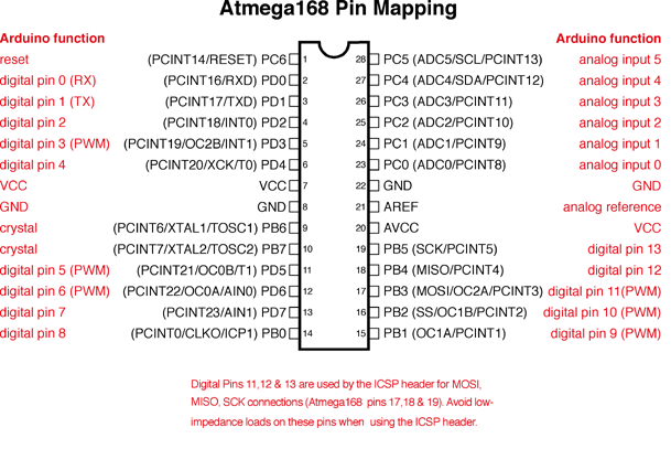
The next pin on the latches that we need to connect is the Output Enable pin. Powering this pin will allow you to actually use the latch and to have it retain its last output value. Again we use the same parallel circuitry, but since we only need 1 pin on the ATMega328 this time it’s a lot less work to do. The pin to use for this one is digital pin 11 and you can see it in the image below as the yellow wires.

The third step is to attach the wiring that ensures the proper latch IC is triggered at the right time. This is where the so called 'clock IC' (74HC138) comes into play. Since the Arduino chip doesn’t have enough output pins to connect them directly, we use the 74HC138 to convert 3 input lines into 8 output lines. How does this work? Well, it’s just a simple binary formula. With 3 bits you can count to 8, so setting those 3 bits at the same time on and/or off will send a small current through the output port that corresponds to that binary number. The pins you need to connect on the ATMega328 are digital pins 8 to 10.

Each of the 8 output pins on the 'clock IC' need to be connected to one of the latch IC’s clock pin. This is a pin that reacts to a drop in current, so when we want to address a certain latch we will have to set that clock pin high, put the data onto the bus and then pull the clock pin low again to actually enable that output.
If you look carefully at the green wires in the image you can see that the output pin 8 is actually located on the other side of the other output pins. It might be easily overlooked when you’re soldering them on. you just go pin 1, pin 2, … until you soldered the wrong pin to the output. Not that I was guilty of doing that, but I certainly had to think twice which pin it was that I needed to skip ![]() .
.
The final step in wiring the brains of this contraption is to connect the transistors that control the layers of our LED cube. In the image below, these are the purple wires. On the ATMega328 you connect them to the analog pins 0 to 5 and the digital pins 12 and 13. These should be the last available pins on the ATMega328 chip.

Now you have all the necessary wiring done and you can get cracking at programming the LED cube. In the next part I’ll discuss how you set up the programming in the Arduino IDE so you can start to create your own cool effects.